Study › Amateur Extra › E6B

E6B

CIRCUIT COMPONENTS

Diodes

Drill results are kept in this browser. Log in to keep them on your account and get a study plan.

E6B011 of 11

What is the most useful characteristic of a Zener diode?

Why A Zener diode is operated in reverse breakdown, where the junction conducts once the reverse voltage reaches the Zener voltage and then holds that voltage nearly fixed even as the current through it changes over a wide range. That flat voltage-versus-current behavior is exactly what a voltage reference or simple shunt regulator needs: a series resistor absorbs the change in supply voltage or load while the diode pins its terminal voltage. Rated Zener voltages run from a couple of volts to a hundred or more, with power dissipation setting the current limit.
Watch out The negative resistance region belongs to the tunnel diode, voltage-variable internal capacitance describes the varactor, and constant current under varying voltage describes a current-regulator diode, not a Zener.
Zener = steady Volts, Varactor = varying C, Tunnel = negative R. Match the diode to its trick.
HamSandwich explanation, first draft. The question and answers are the NCVEC text.
E6B022 of 11

Which characteristic of a Schottky diode makes it a better choice than a silicon junction diode for use as a power supply rectifier?

Why A Schottky diode uses a metal-to-semiconductor junction instead of a P-N junction, so it conducts at roughly 0.2 to 0.3 volts instead of the 0.7 volts typical of silicon. In a rectifier the dissipated power is that forward drop times the load current, so cutting the drop by half a volt means less heat and better supply efficiency, which matters most in high-current, low-voltage supplies. Schottkys also switch fast because they have essentially no minority carrier storage, which helps in switching power supplies.
Watch out The reverse breakdown claim is backwards: Schottky diodes generally have lower reverse voltage ratings than comparable silicon junction diodes, and a constant reverse avalanche voltage describes a Zener. Long carrier retention is also the opposite of the Schottky's near-zero reverse recovery time.
Schottky = short drop: about 0.3 V instead of 0.7 V, so less heat in the rectifier.
HamSandwich explanation, first draft. The question and answers are the NCVEC text.
E6B033 of 11

What property of an LED's semiconductor material determines its forward voltage drop?

Why In an LED, electrons crossing the junction recombine with holes and release their energy as photons. The energy released, and thus the forward voltage needed to push carriers across, is set by the band gap of the semiconductor, the energy separation between the valence and conduction bands. Wider band gap materials emit shorter wavelengths (blue, near 3 V) while narrower ones emit red or infrared (around 1.6 to 1.8 V).
Watch out Junction capacitance is a reverse-bias property that matters in varactors and high-speed switching, not something that sets the forward turn-on voltage; intrinsic resistance only adds a small extra drop at high current.
Band gap sets both the color and the forward voltage: bigger gap means bluer light and higher volts.
HamSandwich explanation, first draft. The question and answers are the NCVEC text.
E6B044 of 11

What type of semiconductor device is designed for use as a voltage-controlled capacitor?

Why A reverse-biased PN junction has a depletion region that acts as the dielectric between two conducting regions, so the junction behaves like a capacitor. Increasing the reverse voltage widens that depletion layer, which increases the plate spacing and lowers the capacitance. A varactor (varicap) diode is built to exploit this effect, and it is commonly used to tune VFOs, PLLs, and to build frequency multipliers.
Watch out A Zener diode also operates reverse biased, which makes it tempting, but it is designed to hold a constant voltage at breakdown for regulation. A tunnel diode provides negative resistance for oscillators, and an SCR is a latching power switch.
Varactor = VARiable reACTOR: more reverse volts, wider gap, less capacitance.
HamSandwich explanation, first draft. The question and answers are the NCVEC text.
E6B055 of 11

What characteristic of a PIN diode makes it useful as an RF switch?

Why A PIN diode has a thick undoped (intrinsic) layer between the P and N regions, which widens the junction and keeps its capacitance very low. Low capacitance means that when the diode is reverse biased or unbiased it looks like a near open circuit even at RF, giving good isolation; forward biased, the stored charge in the intrinsic layer makes it act like a low, current-controlled resistance. That combination of high off-isolation and low on-resistance is exactly what an RF switch or attenuator needs.
Watch out High reverse breakdown voltage and power dissipation are useful ratings in rectifiers and power devices, but they have nothing to do with how cleanly a diode passes or blocks RF; the claim about reverse bias controlling forward voltage drop is not a real diode behavior.
PIN = thick Intrinsic layer = low capacitance = the RF can't sneak across when it's off.
HamSandwich explanation, first draft. The question and answers are the NCVEC text.
E6B066 of 11

Which of the following is a common use of a Schottky diode?

Why A Schottky diode uses a metal-to-semiconductor junction instead of a P-N junction, so there is no stored minority charge to sweep out. That gives it very fast switching, low junction capacitance, and a low forward drop of roughly 0.3 V, which makes it ideal for mixing and detecting signals at VHF, UHF and microwave frequencies where an ordinary silicon junction diode would be too slow.
Watch out The negative-resistance oscillator element is a tunnel diode, voltage-variable capacitance for AFC comes from a varactor, and a constant voltage reference is a Zener diode.
Schottky = metal junction, no charge storage = fast. Think 'Schottky for switching and SHF-speed mixers'.
HamSandwich explanation, first draft. The question and answers are the NCVEC text.
E6B077 of 11

What causes a junction diode to fail from excessive current?

Why Current flowing through a forward-biased junction dissipates power equal to roughly the forward voltage drop times the current, and that power turns into heat right at the tiny junction. If the heat cannot escape through the package and heat sink fast enough, the junction temperature climbs past its rated limit (commonly around 150 C for silicon) and the semiconductor material and its bonds are destroyed. So the current rating of a diode is really a thermal rating in disguise.
Watch out Excessive inverse voltage is a real diode failure mode, but that is reverse breakdown caused by exceeding the peak inverse voltage rating, not by too much forward current.
Too much current equals too much heat: diode current ratings are really heat ratings.
HamSandwich explanation, first draft. The question and answers are the NCVEC text.
E6B088 of 11

Which of the following is a Schottky barrier diode?

Why A Schottky barrier diode is formed where a metal contacts a lightly doped semiconductor rather than by joining P-type and N-type silicon. That metal-semiconductor barrier conducts by majority carriers only, so there is no minority carrier storage time, giving very fast switching and a low forward drop of roughly 0.3 V. That makes Schottky devices favorites for high-frequency detectors, mixers and low-loss rectifiers.
Watch out A PIN junction is a different device entirely, with an undoped intrinsic layer between P and N regions, used as an RF switch or attenuator; the thermionic emission diode is a vacuum tube.
Schottky = metal meets semiconductor: no P-N sandwich, ~0.3 V drop, very fast.
HamSandwich explanation, first draft. The question and answers are the NCVEC text.
E6B099 of 11

What is a common use for point-contact diodes?

Why A point-contact diode is made by pressing a fine metal wire against a semiconductor surface, giving an extremely small junction area. That means very low junction capacitance, so the diode can rectify at VHF, UHF and microwave frequencies where an ordinary PN junction would simply pass the signal through its own capacitance. That speed makes it the classic detector for demodulating or sensing RF, as in the old 'cat's whisker' crystal set and in modern RF probes and power meters.
Watch out Using it as a high-voltage rectifier is the trap: the tiny contact area gives a low reverse breakdown voltage and very little current handling, so it fails in power rectifier service. Constant voltage is a Zener's job, and constant current is what a current-regulator diode does.
Tiny contact, tiny capacitance, fast enough for RF: point-contact means detector, not power rectifier.
HamSandwich explanation, first draft. The question and answers are the NCVEC text.
E6B1010 of 11

In Figure E6-2, which is the schematic symbol for a Schottky diode?
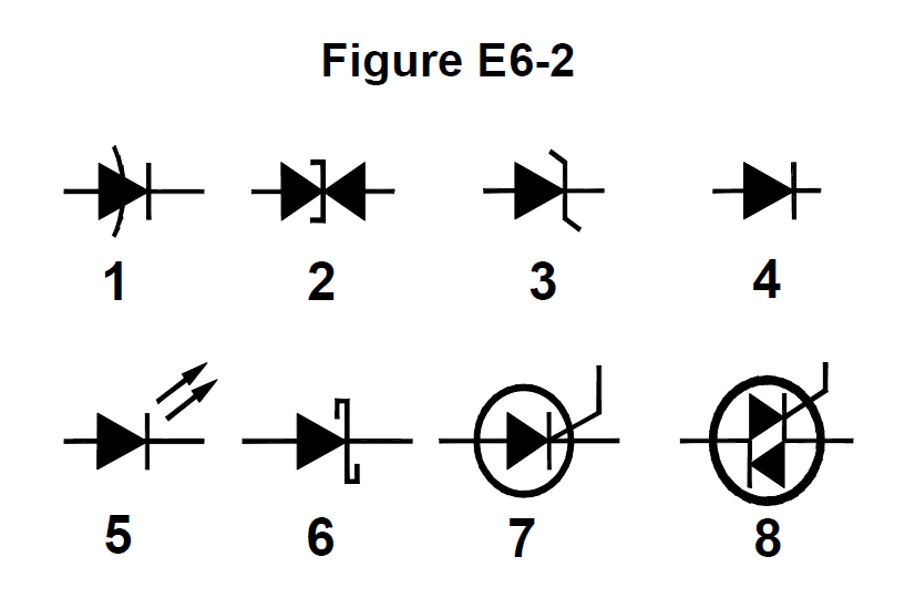
Figure E6-2 from the NCVEC question pool
Why Diode symbols in the figure all share the same triangle-pointing-at-a-bar shape, and the shape of the bar tells you the type. The Schottky diode uses a cathode bar bent into a squared-off S at both ends, matching symbol 6. A Schottky is a metal-to-semiconductor junction rather than a PN junction, which gives it a low forward drop (about 0.3 V) and very fast switching, so it shows up in RF detectors and switching supplies.
Watch out The easy mix-up is the Zener, whose cathode bar is bent at only one end into a Z-like flag; a plain straight bar is an ordinary rectifier diode.
Bar shape names the diode: S-shaped bar = Schottky, Z-shaped bar = Zener, plain bar = ordinary.
HamSandwich explanation, first draft. The question and answers are the NCVEC text.
E6B1111 of 11

What is used to control the attenuation of RF signals by a PIN diode?

Why A PIN diode has a wide undoped intrinsic (I) layer between the P and N regions. At RF the stored charge in that layer does not have time to recombine each cycle, so the diode behaves as a linear resistor rather than a rectifier, and the value of that resistance is set by how much DC current is flowing through it. More forward current means more stored carriers, lower resistance, and less attenuation, so a simple DC control current gives a smooth variable RF attenuator or switch.
Watch out The choice about a large reverse voltage describes how a varactor is operated, where reverse bias sets junction capacitance; reverse biasing a PIN diode just turns it off rather than giving variable attenuation.
PIN = current-controlled resistor. Vary the DC current, vary the RF loss. Varactors use reverse voltage; PINs use forward current.
HamSandwich explanation, first draft. The question and answers are the NCVEC text.
Yaesu FT-65R VHF/UHF Dual Band HandheldSponsored · View on Amazon →ARRL Ham Radio License ManualSponsored · View on Amazon →
← E6A All groups E6C →