Semiconductor materials and devices: semiconductor materials; bipolar junction transistors; operation and types of field-effect transistors
E6A01
In what application is gallium arsenide used as a semiconductor material?
-
A
In high-current rectifier circuits
-
B
In high-power audio circuits
-
C
In microwave circuits
-
D
In very low-frequency RF circuits
E6A02
Which of the following semiconductor materials contains excess free electrons?
-
A
N-type
-
B
P-type
-
C
Bipolar
-
D
Insulated gate
E6A03
Why does a PN-junction diode not conduct current when reverse biased?
-
A
Only P-type semiconductor material can conduct current
-
B
Only N-type semiconductor material can conduct current
-
C
Holes in P-type material and electrons in the N-type material are separated by the applied voltage, widening the depletion region
-
D
Excess holes in P-type material combine with the electrons in N-type material, converting the entire diode into an insulator
E6A04
What is the name given to an impurity atom that adds holes to a semiconductor crystal structure?
-
A
Insulator impurity
-
B
N-type impurity
-
C
Acceptor impurity
-
D
Donor impurity
E6A05
How does DC input impedance at the gate of a field-effect transistor (FET) compare with that of a bipolar transistor?
-
A
They are both low impedance
-
B
An FET has lower input impedance
-
C
An FET has higher input impedance
-
D
They are both high impedance
E6A06
What is the beta of a bipolar junction transistor?
-
A
The frequency at which the current gain is reduced to 0.707
-
B
The change in collector current with respect to the change in base current
-
C
The breakdown voltage of the base-to-collector junction
-
D
The switching speed
E6A07
Which of the following indicates that a silicon NPN junction transistor is biased on?
-
A
Base-to-emitter resistance of approximately 6 ohms to 7 ohms
-
B
Base-to-emitter resistance of approximately 0.6 ohms to 0.7 ohms
-
C
Base-to-emitter voltage of approximately 6 volts to 7 volts
-
D
Base-to-emitter voltage of approximately 0.6 volts to 0.7 volts
E6A08
What is the term for the frequency at which the grounded-base current gain of a bipolar junction transistor has decreased to 0.7 of the gain obtainable at 1 kHz?
-
A
Corner frequency
-
B
Alpha rejection frequency
-
C
Beta cutoff frequency
-
D
Alpha cutoff frequency
E6A09
What is a depletion-mode field-effect transistor (FET)?
-
A
An FET that exhibits a current flow between source and drain when no gate voltage is applied
-
B
An FET that has no current flow between source and drain when no gate voltage is applied
-
C
An FET that exhibits very high electron mobility due to a lack of holes in the N-type material
-
D
An FET for which holes are the majority carriers
E6A10
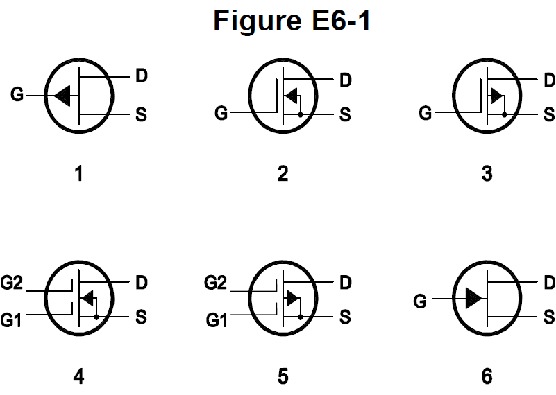
In Figure E6-1, which is the schematic symbol for an N-channel dual-gate MOSFET?
-
A
2
-
B
4
-
C
5
-
D
6
E6A11
In Figure E6-1, which is the schematic symbol for a P-channel junction FET?
-
A
1
-
B
2
-
C
3
-
D
6
E6A12
What is the purpose of connecting Zener diodes between a MOSFET gate and its source or drain?
-
A
To provide a voltage reference for the correct amount of reverse-bias gate voltage
-
B
To protect the substrate from excessive voltages
-
C
To keep the gate voltage within specifications and prevent the device from overheating
-
D
To protect the gate from static damage