E6C01
What is the function of hysteresis in a comparator?
-
A
To prevent input noise from causing unstable output signals
-
B
To allow the comparator to be used with AC input signals
-
C
To cause the output to continually change states
-
D
To increase the sensitivity
E6C02
What happens when the level of a comparator's input signal crosses the threshold voltage?
-
A
The IC input can be damaged
-
B
The comparator changes its output state
-
C
The reference level appears at the output
-
D
The feedback loop becomes unstable
E6C03
What is tri-state logic?
-
A
Logic devices with 0, 1, and high-impedance output states
-
B
Logic devices that utilize ternary math
-
C
Logic with three output impedances which can be selected to better match the load impedance
-
D
A counter with eight states
E6C04
Which of the following is an advantage of BiCMOS logic?
-
A
Its simplicity results in much less expensive devices than standard CMOS
-
B
It is immune to electrostatic damage
-
C
It has the high input impedance of CMOS and the low output impedance of bipolar transistors
-
D
All these choices are correct
E6C05
Which of the following digital logic families has the lowest power consumption?
-
A
Schottky TTL
-
B
ECL
-
C
NMOS
-
D
CMOS
E6C06
Why do CMOS digital integrated circuits have high immunity to noise on the input signal or power supply?
-
A
Large bypass capacitance is inherent
-
B
The input switching threshold is about twice the power supply voltage
-
C
The input switching threshold is about half the power supply voltage
-
D
Bandwidth is very limited
E6C07
What best describes a pull-up or pull-down resistor?
-
A
A resistor in a keying circuit used to reduce key clicks
-
B
A resistor connected to the positive or negative supply used to establish a voltage when an input or output is an open circuit
-
C
A resistor that ensures that an oscillator frequency does not drift
-
D
A resistor connected to an op-amp output that prevents signals from exceeding the power supply voltage
E6C08
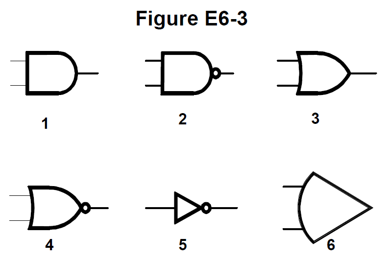
In Figure E6-3, which is the schematic symbol for a NAND gate?
-
A
1
-
B
2
-
C
3
-
D
4
E6C09
What is used to design the configuration of a field-programmable gate array (FPGA)?
-
A
Karnaugh maps
-
B
Hardware description language (HDL)
-
C
An auto-router
-
D
Machine and assembly language
E6C10
In Figure E6-3, which is the schematic symbol for a NOR gate?
-
A
1
-
B
2
-
C
3
-
D
4
E6C11
In Figure E6-3, which is the schematic symbol for the NOT operation (inversion)?
-
A
2
-
B
4
-
C
5
-
D
6